This document was ed by and they confirmed that they have the permission to share it. If you are author or own the copyright of this book, please report to us by using this report form. Report 445h4w
Overview 1s532p
& View Schottky & Ohmic s as PDF for free.
More details 6h715l
- Words: 1,781
- Pages: 33
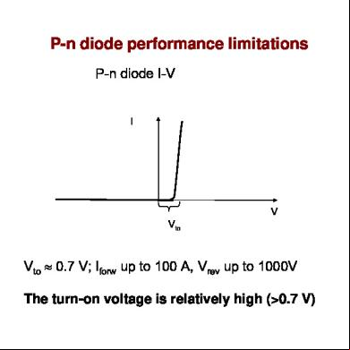
P-n diode performance limitations P-n diode I-V
I
V Vto
Vto ≈ 0.7 V; Iforw up to 100 A, Vrev up to 1000V The turn-on voltage is relatively high (>0.7 V)
1
Switching processes in p-n diodes are relatively slow When a square wave voltage is applied to a p-n diode, it is forward biased duirng one halfcycle and reverse biased during the next half-cycle Under forward bias, the current is
I≈
Vd Vs
R I
Vs
forward
Vs − Vd R reverse
Under reverse bias, the current is almost equal to zero
t
I
t
Using regular p-n diodes, this pulsed current waveform can only be obtained with low frequency pulses
2
Switching processes in p-n diodes (cont.) However, if the pulse frequency is high the reverse current shows significant increase
Vs
t
Vd Vs
I
ideal
R t
I
practical
I
t
Real p-n diode transient at high frequency
High frequency
3
Charge storage and Diode transients
Ln
Lp
Recall the injected carrier distribution at forward bias
-xp
xn
-xp
xn
At reverse bias the steady- state minority carrier concentration is very low. But not immediately after switching from the forward bias!
4
Schottky Diodes Schottky diode has low forward voltage drop and very fast switching speed. Schottky diode consists of a metal - semiconductor junction. There is no p-n junction in Schottky diode.
In 1938, Walter Schottky formulated a theory predicting the Schottky effect.
In Schottky diode, there is no minority carrier injection
metal
semiconductor
5
Band diagrams of p-n and Schottky diodes In Schottky diode, the depletion region occurs only in the semiconductor region as metal has extremely high electron (hole) concentration. EC
EF
EC
EF
EV
p
n
EV
metal
n
6
Schottky Barrier Formation Work function (Φ): Energy difference between Fermi level and vacuum level. It is a minimum energy needed to remove an electron from a solid.
Vaccum level (outside the solid)
Φ
Φ EC
EV
Vaccum level (outside the solid)
Electron Affinity (Xs): Energy difference between the conduction band edge and the vacuum level.
X EC
EV
7
…continued…Schottky Barrier Formation Metal – n-type semiconductor before Vacuum level (outside the solid)
In metals, the conductance band edge EC and the valence band Ev are the same (both at EF level)
Xs
Φs
Φm
EC EFs
EFm
EV
metal
semiconductor
8
…continued…Schottky Barrier Formation After (with n- type material): Vacuum level (outside the solid)
Φm
Xs
Φs EC EF
EV
Schottky barrier for electrons
metal
semiconductor
9
…continued…Schottky Barrier Formation Before (with p-type material): Vacuum level (outside the solid)
Xs
Φs
Φm
EC
EFs
EFm
EV
metal
semiconductor
10
…continued…Schottky Barrier Formation After (with p-type material): Xs
Vacuum level (outside the solid)
Φs
Φm
EC
EFs EV
Schottky barrier for holes
metal
semiconductor
11
Schottky diode characteristics Using energy – voltage relationships: Φm= q φm and Xs = q χs , we can find:
metal
semiconductor
The Schottky barrier height at equilibrium,
φb = φm − χs The built-in voltage, Vbi
qφm qχs qφs
The depletion region charge density,
Vbi = φ m − φs
qVbi
qφbo
EF
ρ = qN d Note: there is no depletion region in metal
EV
The depletion region width,
xn =
2 ε ε 0 Vbi qN d
EC
xn
12
Schottky diode under bias
VR metal
VF
N type
metal
N type
q(Vbi+VR)
EF
xn Reverse bias
N type
q(Vbi-VF)
qVbi
EC
EV
metal
xn
Equilibrium
EC
EC
EF
EF
EV
EV xn Forward bias 13
Schottky diode current Schottky diode has the same type of current - voltage dependence as a p-n diode:
I SCH
⎡ ⎛ qV = I S ⎢exp ⎜ ⎝ kT ⎣
⎞ ⎤ ⎟ − 1⎥ ⎠ ⎦
However, important difference is that in Schottky diodes, the current is NOT associated with electron and hole ACCUMULATION (injection, diffusion and recombination) as in p-n diodes.
q(Vbi-V) EC EF
EV
The current flow mechanism in Schottky diodes is a thermionic emission. The thermionic emission is the process of electron transfer OVER the Schottky barrier 14
…continued…Schottky diode current The saturation current parameter Is in Schottky diodes depends on the Schottky barrier height: ⎛ qφb I s = A T exp ⎜ − ⎝ kBT *
2
⎞ ⎟× A ⎠
A is the diode area. A* is the Richardson’s constant: * 2 4 π qm * nk A = h3
where mn is the electron effective mass, h is the Planck constant and k is the Boltzmann constant. 15
Microwave Schottky diodes
HSCH-9161 Millimeter Wave GaAs Schottky Diode (Agilent)
16
Ohmic s + p-type
n-type
Any semiconductor device has to be connected to external wires in order to form an electronic circuit in combination with other circuit elements. In the case of a p-n diode, for example, s have to be provided to both p-type and n-type regions of the device in order to connect the 17 diode to an external circuit.
Ohmic s Ohmic s must be as low-resistive as possible, so that the current flowing through a semiconductor device leads to the smallest parasitic voltage drop.
Ohmic
⎛ qV ⎞ − 1⎟ xp ⎜ ⎝ kT ⎠
In good Ohmic s, the voltage drop that occurs across the must be low and proportional to the current (so that the s do not introduce any nonlinearities). Since such I-Vs follow the Ohm's law, they are usually called ohmic s.
IS
p-n junction
Ohmic s to semiconductors are often made using Schottky s 18
Rectifying Schottky s n-type semiconductor
n-type
Φ m > Φs
metal
semiconductor
Rectifying Schottky creates an electron depletion region at the metal-semiconductor interface
19
Rectifying Schottky s p-type semiconductor p-type
Φ m< Φ s
metal
semiconductor
Rectifying Schottky creates a hole depletion region at the metal-semiconductor interface
20
Non - rectifying Schottky s
Schottky s (Rectifying s)
Criteria: • n-type Φm> Φs • p-type Φm< Φs
Ohmic s (Non-rectifying s)
Criteria: • n-type Φm< Φs • p-type Φm> Φs
21
Non - rectifying Schottky s Ohmic to n-type semiconductor Φm< Φs
Majority carriers are electrons; there is no potential barrier for electrons in both forward or reverse directions:
Non-rectifying Schottky creates an electron accumulation region at the metal-semiconductor interface. The electron concentration in the region is higher than that in the 22 bulk. The resistance of the region is low.
Non - rectifying Schottky s Ohmic to p-type semiconductor Φm> Φs
Majority carriers are holes; there is no potential barrier for holes in both forward or reverse directions:
Non-rectifying Schottky creates a hole accumulation region at the metal-semiconductor interface. The hole concentration in the region is higher than that in the 23 bulk. The resistance of the region is low.
Ohmic under bias Ohmic to n-type semiconductor
EC EF EV
Positive bias at metal
Negative bias at metal
V metal
N type
V metal
N type
EC EF EC
EV
No barrier, so almost no voltage drop
EF
The voltage is evenly distributed in the bulk
EV
Electron reservoir at the interface
24
…continued…Ohmic under bias Ohmic to p-type semiconductor
EC EF EV
Negative bias at metal
Positive bias at metal
V
V metal
metal
N type
N type
EC
EC
EF
EF
EV
EV
Hole reservoir at the interface
25
Tunneling Schottky s Issue: Not for all semiconductors, it is possible to find the metal with Φm > Φs If the condition Φm > Φs is not met, the Schottky creates a depletion region at the Metal – Semiconductor interface. Solution: heavily doped semiconductor
+
Depletion region width = W EC
EF
EC
EF
1 W~ ND
W Low-doped material – large W
EV
+ -
EV
Highly-doped material – small W
Metal - n-type example Schottky to a heavily doped semiconductor creates a tunneling with very low effective resistance.
26
Tunneling Schottky s for high voltage devices: only sub- regions are heavily doped
Top metal p+ -type material (heavily doped)
n-type material; ND and dn are chosen to provide the required operating voltage
dp
dn
n+ sub- layer
Bottom metal
27
Sub- doping by annealing During high-temperature annealing, metal atoms diffuse into semiconductor and create donor impurities. The material needs to be properly chosen to create donor (acceptor in p-materials) type of impurities. Top metal p+ -type material (heavily doped)
n-type material; ND and dn are chosen to provide the required operating voltage
dp
dn
n+ annealed region
Bottom metal
28
The resistance A quantitative measure of the quality is the specific resistance, ρc, which is the resistance per unit area. sandwich type devices also called “vertical geometry” devices The resistance of each in a sandwich-type structure (“VERTICAL” structure): RCV=ρCV/A, where A is the area. ρCV is specific resistance for vertical structures: [ρCV] = Ω×cm2 Typical current densities in sandwich type devices can be as high as 104 A/cm2. Hence, the specific resistance of 10-5 Ω×cm2 is needed to maintain a voltage drop on the order of 0.1 V. 29
resistance of planar structures W
active layer
Planar, or “lateral geometry” device structure
substrate (device “holder”)
Current In planar structures, resistance is inversely proportional to the width W but no longer proportional to the total area. The current density is larger near the edge. The resistance of planar structures is typically given by the resistance per unit width, Rc1. The lateral resistance RC and unit-width resistance RC1 are related as:
Rc1 RC = W
30
Sheet (per square) resistance of thin films L W
t
The resistance R of a thin semiconductor film between the two s,
L R=ρ tW
For thin films, commonly used thin film characteristic is so called “resistance per square” or “sheet resistance”:
Rsq =
ρ t
L R = R sq W
When L = W, > R = Rsq
31
Transmission Line Model (TLM) method to determining resistance L=1μm
2μm
3μm W t
Resistance Rn,n+1 between two adjacent s in the TLM pattern,
R n ,n +1 = 2R c + R sq
L n ,n +1 W
Where Ln,n+1 is the distance between the s number n and n+1, Rsq is the resistance of the semiconductor film “per square”, 32
From the Y axis intercept we can find the value of RC. From the slope of R (L) plot we can find the film resistance per square:
ΔL ΔR = Rsq W
Resistance (Ω)
Transmission Line Model (TLM) plot
ΔR ΔL
2Rc
Distance between pads L (μm) 33
I
V Vto
Vto ≈ 0.7 V; Iforw up to 100 A, Vrev up to 1000V The turn-on voltage is relatively high (>0.7 V)
1
Switching processes in p-n diodes are relatively slow When a square wave voltage is applied to a p-n diode, it is forward biased duirng one halfcycle and reverse biased during the next half-cycle Under forward bias, the current is
I≈
Vd Vs
R I
Vs
forward
Vs − Vd R reverse
Under reverse bias, the current is almost equal to zero
t
I
t
Using regular p-n diodes, this pulsed current waveform can only be obtained with low frequency pulses
2
Switching processes in p-n diodes (cont.) However, if the pulse frequency is high the reverse current shows significant increase
Vs
t
Vd Vs
I
ideal
R t
I
practical
I
t
Real p-n diode transient at high frequency
High frequency
3
Charge storage and Diode transients
Ln
Lp
Recall the injected carrier distribution at forward bias
-xp
xn
-xp
xn
At reverse bias the steady- state minority carrier concentration is very low. But not immediately after switching from the forward bias!
4
Schottky Diodes Schottky diode has low forward voltage drop and very fast switching speed. Schottky diode consists of a metal - semiconductor junction. There is no p-n junction in Schottky diode.
In 1938, Walter Schottky formulated a theory predicting the Schottky effect.
In Schottky diode, there is no minority carrier injection
metal
semiconductor
5
Band diagrams of p-n and Schottky diodes In Schottky diode, the depletion region occurs only in the semiconductor region as metal has extremely high electron (hole) concentration. EC
EF
EC
EF
EV
p
n
EV
metal
n
6
Schottky Barrier Formation Work function (Φ): Energy difference between Fermi level and vacuum level. It is a minimum energy needed to remove an electron from a solid.
Vaccum level (outside the solid)
Φ
Φ EC
EV
Vaccum level (outside the solid)
Electron Affinity (Xs): Energy difference between the conduction band edge and the vacuum level.
X EC
EV
7
…continued…Schottky Barrier Formation Metal – n-type semiconductor before Vacuum level (outside the solid)
In metals, the conductance band edge EC and the valence band Ev are the same (both at EF level)
Xs
Φs
Φm
EC EFs
EFm
EV
metal
semiconductor
8
…continued…Schottky Barrier Formation After (with n- type material): Vacuum level (outside the solid)
Φm
Xs
Φs EC EF
EV
Schottky barrier for electrons
metal
semiconductor
9
…continued…Schottky Barrier Formation Before (with p-type material): Vacuum level (outside the solid)
Xs
Φs
Φm
EC
EFs
EFm
EV
metal
semiconductor
10
…continued…Schottky Barrier Formation After (with p-type material): Xs
Vacuum level (outside the solid)
Φs
Φm
EC
EFs EV
Schottky barrier for holes
metal
semiconductor
11
Schottky diode characteristics Using energy – voltage relationships: Φm= q φm and Xs = q χs , we can find:
metal
semiconductor
The Schottky barrier height at equilibrium,
φb = φm − χs The built-in voltage, Vbi
qφm qχs qφs
The depletion region charge density,
Vbi = φ m − φs
qVbi
qφbo
EF
ρ = qN d Note: there is no depletion region in metal
EV
The depletion region width,
xn =
2 ε ε 0 Vbi qN d
EC
xn
12
Schottky diode under bias
VR metal
VF
N type
metal
N type
q(Vbi+VR)
EF
xn Reverse bias
N type
q(Vbi-VF)
qVbi
EC
EV
metal
xn
Equilibrium
EC
EC
EF
EF
EV
EV xn Forward bias 13
Schottky diode current Schottky diode has the same type of current - voltage dependence as a p-n diode:
I SCH
⎡ ⎛ qV = I S ⎢exp ⎜ ⎝ kT ⎣
⎞ ⎤ ⎟ − 1⎥ ⎠ ⎦
However, important difference is that in Schottky diodes, the current is NOT associated with electron and hole ACCUMULATION (injection, diffusion and recombination) as in p-n diodes.
q(Vbi-V) EC EF
EV
The current flow mechanism in Schottky diodes is a thermionic emission. The thermionic emission is the process of electron transfer OVER the Schottky barrier 14
…continued…Schottky diode current The saturation current parameter Is in Schottky diodes depends on the Schottky barrier height: ⎛ qφb I s = A T exp ⎜ − ⎝ kBT *
2
⎞ ⎟× A ⎠
A is the diode area. A* is the Richardson’s constant: * 2 4 π qm * nk A = h3
where mn is the electron effective mass, h is the Planck constant and k is the Boltzmann constant. 15
Microwave Schottky diodes
HSCH-9161 Millimeter Wave GaAs Schottky Diode (Agilent)
16
Ohmic s + p-type
n-type
Any semiconductor device has to be connected to external wires in order to form an electronic circuit in combination with other circuit elements. In the case of a p-n diode, for example, s have to be provided to both p-type and n-type regions of the device in order to connect the 17 diode to an external circuit.
Ohmic s Ohmic s must be as low-resistive as possible, so that the current flowing through a semiconductor device leads to the smallest parasitic voltage drop.
Ohmic
⎛ qV ⎞ − 1⎟ xp ⎜ ⎝ kT ⎠
In good Ohmic s, the voltage drop that occurs across the must be low and proportional to the current (so that the s do not introduce any nonlinearities). Since such I-Vs follow the Ohm's law, they are usually called ohmic s.
IS
p-n junction
Ohmic s to semiconductors are often made using Schottky s 18
Rectifying Schottky s n-type semiconductor
n-type
Φ m > Φs
metal
semiconductor
Rectifying Schottky creates an electron depletion region at the metal-semiconductor interface
19
Rectifying Schottky s p-type semiconductor p-type
Φ m< Φ s
metal
semiconductor
Rectifying Schottky creates a hole depletion region at the metal-semiconductor interface
20
Non - rectifying Schottky s
Schottky s (Rectifying s)
Criteria: • n-type Φm> Φs • p-type Φm< Φs
Ohmic s (Non-rectifying s)
Criteria: • n-type Φm< Φs • p-type Φm> Φs
21
Non - rectifying Schottky s Ohmic to n-type semiconductor Φm< Φs
Majority carriers are electrons; there is no potential barrier for electrons in both forward or reverse directions:
Non-rectifying Schottky creates an electron accumulation region at the metal-semiconductor interface. The electron concentration in the region is higher than that in the 22 bulk. The resistance of the region is low.
Non - rectifying Schottky s Ohmic to p-type semiconductor Φm> Φs
Majority carriers are holes; there is no potential barrier for holes in both forward or reverse directions:
Non-rectifying Schottky creates a hole accumulation region at the metal-semiconductor interface. The hole concentration in the region is higher than that in the 23 bulk. The resistance of the region is low.
Ohmic under bias Ohmic to n-type semiconductor
EC EF EV
Positive bias at metal
Negative bias at metal
V metal
N type
V metal
N type
EC EF EC
EV
No barrier, so almost no voltage drop
EF
The voltage is evenly distributed in the bulk
EV
Electron reservoir at the interface
24
…continued…Ohmic under bias Ohmic to p-type semiconductor
EC EF EV
Negative bias at metal
Positive bias at metal
V
V metal
metal
N type
N type
EC
EC
EF
EF
EV
EV
Hole reservoir at the interface
25
Tunneling Schottky s Issue: Not for all semiconductors, it is possible to find the metal with Φm > Φs If the condition Φm > Φs is not met, the Schottky creates a depletion region at the Metal – Semiconductor interface. Solution: heavily doped semiconductor
+
Depletion region width = W EC
EF
EC
EF
1 W~ ND
W Low-doped material – large W
EV
+ -
EV
Highly-doped material – small W
Metal - n-type example Schottky to a heavily doped semiconductor creates a tunneling with very low effective resistance.
26
Tunneling Schottky s for high voltage devices: only sub- regions are heavily doped
Top metal p+ -type material (heavily doped)
n-type material; ND and dn are chosen to provide the required operating voltage
dp
dn
n+ sub- layer
Bottom metal
27
Sub- doping by annealing During high-temperature annealing, metal atoms diffuse into semiconductor and create donor impurities. The material needs to be properly chosen to create donor (acceptor in p-materials) type of impurities. Top metal p+ -type material (heavily doped)
n-type material; ND and dn are chosen to provide the required operating voltage
dp
dn
n+ annealed region
Bottom metal
28
The resistance A quantitative measure of the quality is the specific resistance, ρc, which is the resistance per unit area. sandwich type devices also called “vertical geometry” devices The resistance of each in a sandwich-type structure (“VERTICAL” structure): RCV=ρCV/A, where A is the area. ρCV is specific resistance for vertical structures: [ρCV] = Ω×cm2 Typical current densities in sandwich type devices can be as high as 104 A/cm2. Hence, the specific resistance of 10-5 Ω×cm2 is needed to maintain a voltage drop on the order of 0.1 V. 29
resistance of planar structures W
active layer
Planar, or “lateral geometry” device structure
substrate (device “holder”)
Current In planar structures, resistance is inversely proportional to the width W but no longer proportional to the total area. The current density is larger near the edge. The resistance of planar structures is typically given by the resistance per unit width, Rc1. The lateral resistance RC and unit-width resistance RC1 are related as:
Rc1 RC = W
30
Sheet (per square) resistance of thin films L W
t
The resistance R of a thin semiconductor film between the two s,
L R=ρ tW
For thin films, commonly used thin film characteristic is so called “resistance per square” or “sheet resistance”:
Rsq =
ρ t
L R = R sq W
When L = W, > R = Rsq
31
Transmission Line Model (TLM) method to determining resistance L=1μm
2μm
3μm W t
Resistance Rn,n+1 between two adjacent s in the TLM pattern,
R n ,n +1 = 2R c + R sq
L n ,n +1 W
Where Ln,n+1 is the distance between the s number n and n+1, Rsq is the resistance of the semiconductor film “per square”, 32
From the Y axis intercept we can find the value of RC. From the slope of R (L) plot we can find the film resistance per square:
ΔL ΔR = Rsq W
Resistance (Ω)
Transmission Line Model (TLM) plot
ΔR ΔL
2Rc
Distance between pads L (μm) 33
Related Documents 2w1qw
October 2022 0

Ohmic Heating 6k5542
November 2021 0
Ohmic Heating 6k5542
October 2019 146
s 14422y
April 2020 82
Schottky Diode 633x1d
March 2021 0
s 14422y
October 2019 203More Documents from "Archana Tripathi" 1z6k18
October 2022 0

11th Std-computer Applications Vol-ii Em - Www.tn11th.in 4w421u
August 2021 0
Mango 453y6x
March 2021 0
Case Study 3m2j30
December 2019 70
Latest Advancements In Microprocessor 611xu
November 2019 46
December 2019 59